
Recently added item(s)
Sputtering Targets Plasma Etching is a process in which particles are ejected from a solid target material due to
bombardment of the target by energetic particles ie. plasma high energtic. In which when the kinetic energy of
the incoming particles is much higher than conventional thermal energies. This process can lead, during
prolonged ion or plasma bombardment of a material, to significant erosion of materials. Sputtering is a
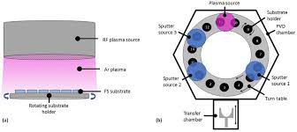
technique used to deposit thin films of a material onto a surface. by first creating a gaseous plasma and then
accelerating the ions from this plasma into some source material, the source material is then eroded by the
arriving ions via energy transfer and is ejected in the form of neutral particles due to elastic or inelastic celliscon
neutral particles – either individual atoms, clusters of atoms or molecules.
Plasma Etching
Sputtering Targets For Plasma Etching is a plasma process which is used to remove small amounts of material
from a surface. It is the only viable method for a lot of applications because the requirement of anisotropic
etching. Anisotropic etching is etching in just one axis for example right down into a trace without etching the
side walls. Plasma etching can also be selective which means that it removes one material but leaves the
other unaffected. Sputtering is removal of atoms caused by high energetic ions hitting the surface, this process
is highly anisotropic. Chemical etching is isotropic. Ion energy-driven etching occurs in plasmas were both
chemical etchants and high energy ions are supplied to the surface. Ion energy-driven etching has a much
higher etch rate then chemical etching and sputtering alone. These results in a anisotropic etching with high
etch rate.
Sputtering Targets Plasma Etching: Applications In Thin Films
The modern methods of plasma-assisted physical vapor deposition techniques provide great flexibility for
designing films with specific chemistry and micro structure, leading to coatings with unique properties.
Ceramic coatings deposited on metallic substrates have shown excellent improvement of the surface
properties, such as a low friction coefficient and a high degree of hardness with associated good wear resistance
and also corrosion resistance to aggressive environments In general, it may be observed that the residual compressive stresses, determined using the curvature method, and increased with the energy parameter, pinholes or defects are usually localized at the grain boundaries, which are defined by the crystal growth process, which consequently models the final film structure.
Sputtering Targets Plasma Etching: Applications
Sputtering Targets For Plasma Etching coating technology is used for thin film deposition of target material on
the desired surface called substrate. In sputter coating a target is bombarded with heavy gas atoms. Metal
atoms ejected from the target by the ionized gas cross the plasma to deposit onto any surface, and this process
is used to form a desired coating on the substrate. physical vapor deposition technique used in application
such as optoelectronics (Solar cell, photodiodes, liquid crystal display-LCD, electronics). The memory
technology(For E.g. laser discs, magneto-optical Media), the surface protection ( tools, machine parts) or the
barrier technology( diffusion barries for e.g. in flexible packing).
The Sputtering Targets For Plasma Etching market based on material type (pure material, alloy and
compounds) by substrate type (Ceramic, Metal & dielectric, Glass, Plastic, Textile and Others, Automotive &
Transport, Architecture, Microelectronics, Data storage, Electronics, Display, Energy, Lighting, Medical, Defense
& Security, Optical Coating, tribological coating, decorative coating and others).