
Recently added item(s)
Silver Nano Particle Ink: Printed electronics will bring to the consumer level great breakthroughs and unique
products in the near future, shifting the usual paradigm of electronic devices and circuit boards from hard boxes
and rigid sheets into flexible thin layers and bringing disposable electronics, smart tags, and so on. The most
promising tool to achieve the target depends upon the availability of nanotechnology-based functional inks. A
certain delay in the innovation-transfer process to the market is now being observed. Nevertheless, the most
widely diffused product, settled technology, and the highest sales volumes are related to the silver
nanoparticles-based ink market, representing the best example of commercial nanotechnology today.
Nano Dimensions provides conductive inks specifically tailored for use in antennas, including radio-frequency
identification (RFID) technology for a variety of devices including smart cards, various ID products, arrays and
more. The Nanoshel family of silver nanoparticles inks, deposited by contactless, digital, inkjet printing, delivers
outstanding results.
Nano Dimension has also developed a suite of dielectric inks to meet the advanced needs of the electronics
community. The insulating properties of these materials are just as important and advanced as the conductive
properties of the conductive inks. For electronic circuits to function properly, properties relating to interference,
adhesion, thermal dissipation and flammability have to be engineered into the ink. Our one-part nano-epoxy
insulating dielectric material provides solutions suited for both rigid and flexible circuits.
Probably the first nanotechnology ever discovered and applied was that of black ink based on carbon black and
bone black, containing fullerenes and a wide variety of aromatic small molecules. Today, printing technology has
expanded its horizon toward the realization of electron devices on any substrate, according to two main
approaches: 1) analog printing, involving the use of linear/rotary machines that are able to realize multiple
copies of the same pattern at a rather high speed (serigraphy, gravure, offset, flexography), involving generally
micro structured inks; and 2) digital printing, where raster machines realize at rather slow speed a single copy of
a pattern that could be changed simply working at the software level (inkjet printing, 3-D printing), involving
nanostructured inks.
In order to exploit the potential of metal NPs fully and to provide effective strategies to tune electronic and
optical properties of materials, the control of size and morphology of nanostructures are of fundamental and
technological interest.60 Noble metal NPs (Ag, Au, Pt) are extremely interesting because of their unique
properties, and among them Ag possess the highest electrical and thermal conductivity, along with other
properties, which promote its extensive use in a wide range of applications. Nowadays, Ag NPs are largely used
to produce conductive tracks with inkjet printing, thanks to the high conductivity and thermal stability of such
materials
Conductive inks normally are aqueous or organic solvent dispersions of silver NPs that are stabilized by
surfactants and polymers that undergo printing, a drying step, and at the end a sintering process that is
commonly achieved by heating the printed substrates to a temperature usually higher than 200°C. Alternatively,
more unconventional techniques, such as microwave, laser radiation, flash sintering, plasma and electrical- or
chemical-induced sintering, can be pursued.
Sintering at 200°C is much below the melting point of silver (960°C), and it can be attributed to the enhanced
surface diffusion of atoms and to surface premelting; therefore, even in the sintering process, the dimension and
shape of Ag NPs are one of the first properties to be investigated.
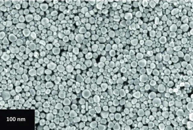
Ag NPs used for inks generally have spherical shape with diameters ranging from 5 to approximately 100 nm
with narrow dimensional distribution. Several works are presented in the literature using such NPs. Fuller et al
described an inkjet ink based on colloidal silver NPs of spherical shape with a diameter of approximately 5–7 nm
dispersed 10 wt% in ?-terpineol, which was sintered at 300°C on a hot plate, giving conductive lines of 80 µm
and presenting a resistivity of 3 µ?/cm.
Ag-based inks for inkjet-printing flexible electronics
Concentrated silver NPs are well-recognized materials with potential applications in the field of printing
technology. These are used for the preparation of metallic structures on various substrates, because of their high
electrical conductivity and resistance to oxidation. Such inks should meet some important requirements: for
instance, they should not dry out and clog when in the print-head, they should have good adhesion to the
substrate with limited coffee-ring effect and reduced particle aggregation, and they should be characterized by
suitable viscosity and surface tension, as they determine drop size, drop-placement accuracy, satellite formation,
and wetting of the substrate. These requirements are very well met by Ag NP-based inks.