
Recently added item(s)
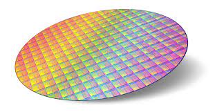
Silicon Wafers is the second most common element on Earth and it is the seventh-most common element in
the entire universe. It is the most common semi conductor and the most widely used in the electronic and
technology sector. There are different silicon fabrication methods including the horizontal gradient freeze
method, the horizontal Bridgeman method, the vertical Bridgeman method, the vertical gradient freeze and
finally the Czochralski pulling method.
Silicon Wafers
During the growth process to obtain the derived purity, different intentional dopants are added. These
introduced impurities can change the electrical properties of the silicon, which can be useful depending on what
the silicon is ultimately being produced for. Boron, aluminum, nitrogen, gallium and indium are just some of the
silicon dopants that can be introduced during the growth process. Depending on what level the silicon has been
doped, the semiconductor can be considered extrinsic or degenerate. Extrinsic would be lightly to moderately
doped whereas degenerate semiconductors act more as conductors because of the high levels of doping that
occurs during the fabrication.
Silicon wafers are a key component in integrated circuits. Integrated circuits are, simply put, a composite of
various electronic components that are arranged to perform a specific function. Silicon is the principle platform
for semiconductor devices. A wafer is a thin slice of this semiconductor material, which serves as the substrate
for microelectronic devices built in and over the wafer
Types of Wafer Substrates
• Single Element Semiconductors
Silicon, Si is the most common semiconductor having atomic number 14, energy gap Eg = 1.12 eV, indirect band
gap; crystal structure-diamond, lattice constant-0.543 nm, thermal conductivity 1.31 W/cm-oC, melting point
1414 oC due to these properties ingle crystal Si can be processed into wafers up to 300 mm in diameter and
having excellent mechanical properties in MEMS applications.
• Silicon on Insulator (SOI)
Only a thin layer on the surface of a silicon wafer is used for making electronic components; the rest serves
essentially as a mechanical support. The role of SOI is to electronically insulate a fine layer of monocrystalline
silicon from the rest of the silicon wafer. Integrated circuits can then be fabricated on the top layer of the SOI
wafers using the same processes as would be used on plain silicon wafers. The embedded layer of insulation enables the SOI-based chips to function at significantly higher speeds while reducing electrical losses. The result is an increase in performance and a reduction in power consumption. There are two types of SOI wafers. Thin
film SOI wafers have a device layer 1.5 m
Wafer bonding. – In this process the surface of two wafers are coated with an insulating layer (usually oxide). The
insulating layers are then bonded together in a furnace creating one single wafer with a buried oxide layer (BOX)
sandwiched between layers of semiconductor. The top of the wafer is then lapped and polished until a desired
thickness of semiconductor above the BOX is achieved.
SIMOX – Separation by Implantation of Oxide. In this process a bulk semiconductor wafer is bombarded with
oxygen ions, creating a layer of buried oxide. The thickness of intrinsic semiconductor above the box is
determined by the ion energy. Anneal reinforces Si-O bonds in the BOX.
Smart Cut – The wafer bonding method is used to form the BOX, but instead of lapping off excess
semiconductor (which is wasteful) a layer of hydrogen is implanted to a depth specifying the desired active layer
of semiconductor. Anneal at ~500 oC splits the wafer along the stress plane created by the implanted hydrogen.
The split wafer may then be reused to form other SIO wafers.
• III-V Semiconductors
Gallium Arsenide (GaAs): After silicon second the most common semiconductor is GaAs having energy gap Eg
= 1.43 eV, direct band gap; crystal structure – zinc blend, thermal conductivity 0.46 W/cm-oC, thermally unstable
above 600 oC. Due to evaporation they does not form sufficient quality native oxide and mechanically fragile.
Due to direct band gap commonly used to fabricate light emitting devices. Because of higher electron and hole
mobilities, use for the variety of high-speed electronic devices. The band gap can be readily engineered by
forming ternary compounds based on GaAs, e.g. AlGaAs.
Gallium Nitride (GaN): The wide band gap of III-V semiconductor with direct bandgap 3.5 eV wide; among very
few semiconductors capable of generating blue radiation. GaN is used for blue LEDs and lasers; intrinsically ntype semiconductor but can be doped p-type. GaN is formed as an epitaxial layer. The Lattice mismatch remains
a problem, creating a high defect density. Incorporation of Indium (InxGa1-xN) allows control of emission from
green to violet (high and low In content respectively). GaN can also be used in UV detectors that do not respond
to visible light. GaN has a Wurtzite(W) or Zinc Blend(ZB) crystal structure
Gallium Phosphide (GaP): The properties of GaP like Crystal structure zinc blend; Lattice constant [A] 5.45;
Density [g/cm3] 4.14; Melting point [oC] 1457, due to these properties of GaP the wafers are used in
Semiconductor industry
Silicon carbide (SiC): The semiconductor featuring energy gap Eg = 2.9 -3.05 eV (wide band gap semiconductor),
indirect band gap; SiC can be obtained in several polytypes- most common hexagonal in the form of either 4H
or 6H polytypes; parameters vary depending on polytype; Intrinsically n-doped; p-type doping and n-type
conductivity control can be obtained by doping with aluminum and nitrogen respectively. SiC features higher
than Si and GaAs electron saturation velocity; excellent semiconductor but difficult and expensive to fabricate
single-crystal wafers; excellent for high power, high temperature applications; SiC is closely lattice matched to
GaN, has a thermal expansion coefficient close to GaN, and is available in both conductive and semi-insulating
substrates. Thus it is often used as a substrate for GaN epitaxial layers. SiC wafers 75 mm in diameter are
available commercially
• Fiber Optic
Silicon is the most economical IR material available. Both P-type and N-type substrates are acceptable for IR
optics provided that they offer transmission greater than 50% in the 1.5 to 6 micron wavelength. Generally
speaking, for N-type, the resistivity should be greater than 20 ohm-cm and, for P-type, greater than 40 ohm-cm.
For use in the near IR, this is not so critical, but for applications for the far IR, resistivity can be critical. Float Zone
Silicon most always meets criteria for optical use.
Uses of Silicon Wafers
Silicon wafers primary use is in integrated circuits. Integrated circuits power many of the devices that modern
society uses every day. Computers and smart phones are just two of the devices that are dependent on this
technology. Although other semiconductors have been tested overtime, silicon has proved to be stable option.
Other uses include sensors, such as the tire pressure sensor system, and solar cells. Silicon wafers absorb the
photons in sunlight and this in turn creates electricity. Silicon wafers are also used for various coating
applications of nanomaterials such as biosensing.